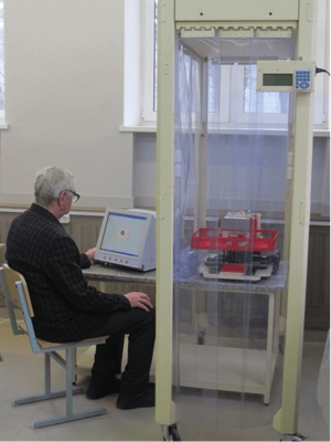
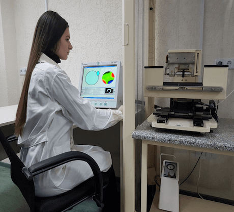
Magnetic-Abrasive Superfine Polishing: example of superfine polishing of parts of optics, lasers and electronics
Problem relevance
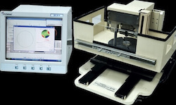
The problem of surfacing with nanoscale relief (Ra < 0.5 nm) and near-surface layers forming with a minimal amount of structural defects is of the most immediate interest to the heavy duty details of the optical, laser and electronic equipment. Surface-finishing improvement affects:
- the optical systems resolution and microoptics performance capabilities
- progress in the development of powerful and compact lasers, scope and effectiveness of their application in various fields
- reduced dimentions of elements and devices for micro- and nanoelectronics
The industry circumstances
The traditional finishing technology for precision surfaces of optical lenses, single crystals – optically active elements of laser devices and wafers for integrated circuits is realized with grinding by wheels with fixed abrasive grains and with subsequent polishing by pastes or suspensions. The grinding wheels application provides hard contact with the treated surface. The high local temperature (up to 2000°C) and high normal pressure values are in the contact zone during processing. Under these conditions the surface layer is formed with a large number of structural defects. The layer depth is 25...75 μm. This layer is removed later by a number of polishing operations using free (unfixed) abrasive grains.
Currently the single crystal wafer and optical glasses are treated by the traditional method with the grinding powder – polishing pads and diamond pastes. This technology is time-consuming and very expensive. The polishing costs compose a considerate share (30% and over) of the wafer-plate cost. The best technology modes provide surface relief with roughness height of 2...5 nm. Finishing methods of chemical and mechanical surface treatment are also widely used in modern production (such as chemical etching, chemical-mechanical polishing, etc.). However, these methods are time-consuming and have limited technological capabilities, besides their use is associated with the environmental and economic problems of usage and recycling of large amounts of chemically aggressive acids and alkalis.
Today, there are only a few large companies with scientific and technical potential and sufficient production capacity worldwide, which are capable of mass-producing high-precision equipment for finishing of precision surfaces of parts for optics, electronics and laser optics: «Satisloh» (Germany), «Optotech» (Germany), «Speed Fam» (the USA), «Lapmaster» (England), «Fujikoshi» (Japan) and others.
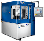
In recent years, the magnetorheological finishing (MRF) technologies have widely spread at finish machining of optics and lasers elements. The MRF principles were developed in Belarus but the development has not been brought to the industrial application for lack of financial resources. The MRF technology was developed in the USA with more than 10 million US dollars investing. Nowadays the QED Company (USA) offers the MRF technology to the world market. The QED has a monopoly on the production of equipment and assistive technology environments. This technology provides the surface roughness in the range of Ra = 1...2 nm and shape accuracy of 6...10 nm.
However, the application of MRF technology is highly complicated because of unstable and nondurable magnetorheological suspension used as the polishing medium. In addition, the cost of QED system and interconnected monitoring equipment exceeds 400 thousand US dollars. The technological media-suspensions cost is about 500 US dollars per 1 liter. These costs are clearly overestimated and unpurchaseable for the majority of potential consumers. The MRF technology features of maintenance and economic factors significantly limit the scope of its industrial application. You can find out here more about comparison of MRF and MAM technologies.
Examples
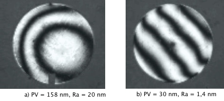
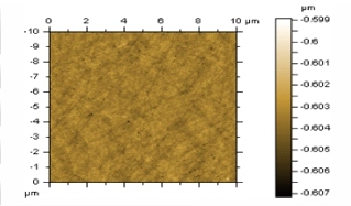
|
ISO 25178 Height Parameters | |
|---|---|---|
| Sq | 0.000369 μm | |
| SSk | -0.256 | |
| Sku | 4.04 | |
| Sp | 0.00458 μm | |
| Sv | 0.00366 μm | |
| Sz | 0.00824 μm | |
| Sa | 0.000272 μm | |
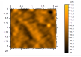
|
ISO 25178 Height Parameters |
|
|---|---|---|
| Sq | 0.189 mm | |
| SSk | 0.137 | |
| Sku | 3.76 | |
| Sp | 1.13 nm | |
| Sv | 0.735 nm | |
| Sz | 1.87 nm | |
| Sa | 0.142 nm | |
