
Polishing of details of optics and electronics
- Computer controlled polishing process based upon Magnetic-Abrasive Machining (MAM)
- Computer controlled magnetic-abrasive polishing technology
- Developed by Polimag
- Equipment samples
- Basic characteristics of models 3905 and MAP-300
- Technology of magnetic-abrasive polishing high-precision flat surfaces
- CaF2 after MAM
- Macrogeometry of Si-Wafer after MAM
- Nanorelief of Si-Wafer Surface after MAM
- Roughness of Si-Wafer Surface after MAM
- Polishing is performed by the shear stresses in the tool material while keeping normal stresses minimal, which results in minimal subsurface damage.
- The usage of magnetic field facilitates polishing of many monocrystal materials because of the magnetoplastic effect.
- The machine allows to reduce peak-to-value figure error 3-4 times for single polishing iteration.
- The index of nanorelief polished surface is Ra < 2 nm
- The process is very simple and expects a low-cost equipment. It is 3-5 times cheaper comparing to available commercial analogues and it is not inferior to them in its technological potential.
- diameter of polished parts - under 200 mm;
- time of polishing, min - 2…15
- power input, kWt - 1.5
- overall dimensions of setup L x B x H, mm : 700 x 600 x 500
- mass of setup - 80 kg
- plates of silicon mono-crystals (substrate of integrated circuits),
- optical glasses,
- fluorides of barium, calcium and magnesium (optically active elements of power laser devices)
- Polishing is performed by the shear stresses in the tool material while keeping normal stresses minimal, which results in minimal subsurface damage.
- The usage of magnetic field facilitates polishing of many monocrystal materials because of the magnetoplastic effect.
- The index of nanorelief polished surface is Ra < 2 nm
- The process is very simple and expects a low-cost equipment. It is 3-5 times cheaper comparing to available commercial analogues and it is not inferior to them in its technological potential.
- diameter of polished parts, mm - 20...200
- thickness of polished parts, mm - < 5
- time of polishing, min - 2...15
- power input, kWt - 1.5
- overall dimensions of setup L x B x H, mm : 700 x 700 x 500
- mass of setup - 80 kg
Computer controlled polishing process based upon Magnetic-Abrasive Machining (MAM)
Areas of application: polishing of precise optics, including convex and slight concave spheres and aspheres.
Description: Process joins the minimal surface roughness and subsurface damage which is well known for MAM with figuring ability. Figuring is performed by scanning surface (previously measured) wcith small removal spot according to calculated kinematics. Kinematics is calculated using specialy developed deconvolution algorithm. A new type of magnetic inductor based on permanent xmagnets can perform xmachining of nonferromagnetic parts of arbitrary size, not jsut thin plates. Soft magnetic abrasive instrument adapts to the macroscopuc shape of surface to be polished.
Current progress: The main process' components were developed. The process has been xtested on flat surfaces. A simple experimental machine with 2-axes positioning system was developed. Achived surface roughness is 1.4 nm Ra for BK7 optical glass. Achived maximum initial MRR is 5 μ/min at spot maximum for BK7 optical glass.
 |  |
| 20 s duration spot using fumed silica | 5 s duration spot using cerium oxide |
| Figure 1: Removal spots for 14mm flat part from BaK4 optical glass | |
|
|
| Figure 2: Flat surface of 14mm part from BaK4 optical glass before (a) and after 195 seconds of polishing run (b) | |
Computer controlled magnetic-abrasive polishing technology
Technology is intended for correction of polished optical surface figure errors. Correction technique is automatic surface scanning with elastic tool which has reproducible influence function.
Features and advantages :
Technical characteristics :
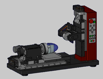
Figure 3: Computer controlled magnetic-abrasive polishing technology
Developed by Polimag
Polimag has developed the technology and created the samples of the equipment for the polishing in the magnetic field of flat precision surfaces of the details from different materials.
Finishing magnetic-abrasive polishing of:
provides the formation of surface nanorelief with the roughness height less than 20 angstrom, that corresponds to the best world samples.
Equipment samples


Basic characteristics of models 3905 and MAP-300
| Diameter of the polished plates, mm | up to 300 |
| Power consumption, kWt | 2.0 |
| Thickness of plates, mm | up to 10 |
| Parameters of power line: | |
| voltage, V | 220 |
| frequency, Hz | 50 |
| Characteristic of roughness of the polished surface Ra, nm | < 2nm |
| Dimensions: length x width x height, m | 1.0 x 0.7 x 1.3 |
| Weight, kg | 250 |
Technology of magnetic-abrasive polishing high-precision flat surfaces
The setup model MA08.01 is used for superthin polishing of high-precision flat parts surfaces of optics, electronics and laser technics.
Features and advantages :
Technical characteristics :
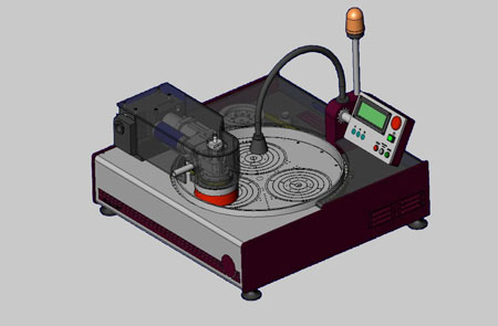
Figure 4: Model MA08.01
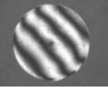
CaF2 after MAM

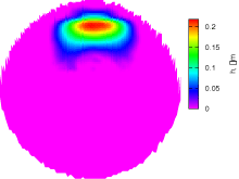
Macrogeometry of Si-Wafer after MAM

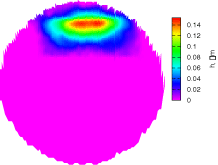
Nanorelief of Si-Wafer Surface after MAM

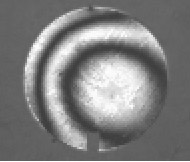
Roughness of Si-Wafer Surface after MAM
